研究方向 Research

四个相互支撑的研究方向:微观机理与计算设计、极限材料制备、极端条件表征、器件与系统应用。

Four interconnected directions: microscopic theory & computational design, extreme material synthesis, characterization under extreme conditions, and devices-to-systems applications.

Microscopic Energy Transport: Theory & Simulation
01

能量输运微观机理与计算设计

Microscopic Energy Transport: Theory & Simulation

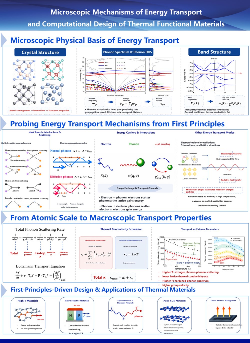
从原子结构出发,用第一性原理与玻尔兹曼输运方程定量预测能量如何穿过材料与界面。

Starting from atomic structures, we use first-principles calculations and the Boltzmann transport equation to quantitatively predict how energy traverses materials and interfaces.

围绕“能量在固体中如何输运”这一基本问题,从声子散射、电子-声子耦合、界面透射三个层面建立定量的微观理论:揭示砷化硼中三/四声子散射竞争导致的高压反常导热行为(Nature 2022);建立界面热导的“实验-扩散失配模型-分子动力学”闭环,实现界面声子透射的定量预测;发展电场驱动电荷重分布的化学键级热导调控理论(Science 2023);并覆盖从弹道到扩散的跨尺度非傅里叶输运。计算设计链“DFT → 声子 BTE → MD/机器学习势 → 原位实验验证”贯通预测与测量。

Centered on the fundamental question of how energy transports in solids, we build quantitative microscopic theories across three levels: phonon scattering, electron-phonon coupling, and interfacial transmission. We revealed the anomalous high-pressure thermal conduction in boron arsenide arising from competing three- and four-phonon scattering (Nature 2022); established an experiment–DMM–MD closed loop for quantitative prediction of interfacial phonon transmission; developed a bond-level thermal tuning theory driven by electric-field-induced charge redistribution (Science 2023); and covered cross-scale non-Fourier transport from ballistic to diffusive regimes. Our design chain — DFT → phonon BTE → MD/machine-learning potentials → in-situ experimental validation — connects prediction with measurement.
Extreme Thermal Materials: Synthesis & Crystal Growth
02

极限热材料制备与生长

Extreme Thermal Materials: Synthesis & Crystal Growth

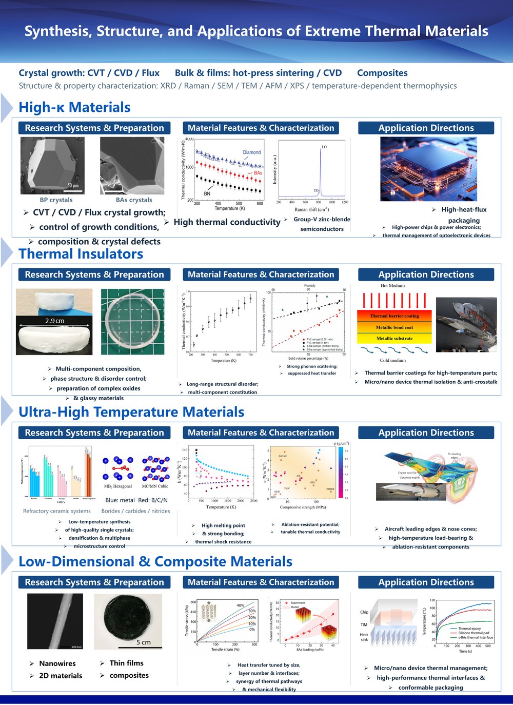
生长与制备覆盖“最高导热—最强耐温—最低导热”三个极限的热材料体系。

We grow and synthesize thermal materials at three extremes: highest conductivity, highest temperature tolerance, and lowest conductivity.

面向极限热功能的三类材料体系:(1)高导热半导体——化学气相输运生长砷化硼单晶,室温热导率约 1300 W/m·K、仅次于金刚石(Science 2018),同位素富集进一步抑制声子散射;(2)超高温陶瓷——改进助熔剂法在温和温度合成 ZrB₂/HfB₂ 硼化物单晶,熔点逾 3000 °C,面向高超声速热防护与聚变极端热载;(3)低维与复合材料——一维磷化硼纳米线、冰模板取向砷化硼复合热界面材料,兼顾高导热与低模量(Nat. Commun. 2021)。

We pursue three classes of materials for extreme thermal functions: (1) High-conductivity semiconductors — boron arsenide single crystals grown by chemical vapor transport, reaching a room-temperature thermal conductivity of ~1300 W/m·K, second only to diamond (Science 2018), with isotope enrichment further suppressing phonon scattering; (2) Ultra-high-temperature ceramics — ZrB₂/HfB₂ boride single crystals synthesized at mild temperatures via a modified flux method, with melting points above 3000 °C for hypersonic thermal protection and fusion heat loads; (3) Low-dimensional & composite materials — 1D boron phosphide nanowires and ice-templated aligned BAs composite thermal interface materials combining high conductivity with low modulus (Nat. Commun. 2021).

Thermal Characterization under Extreme Conditions
03

极端条件热物性表征

Thermal Characterization under Extreme Conditions

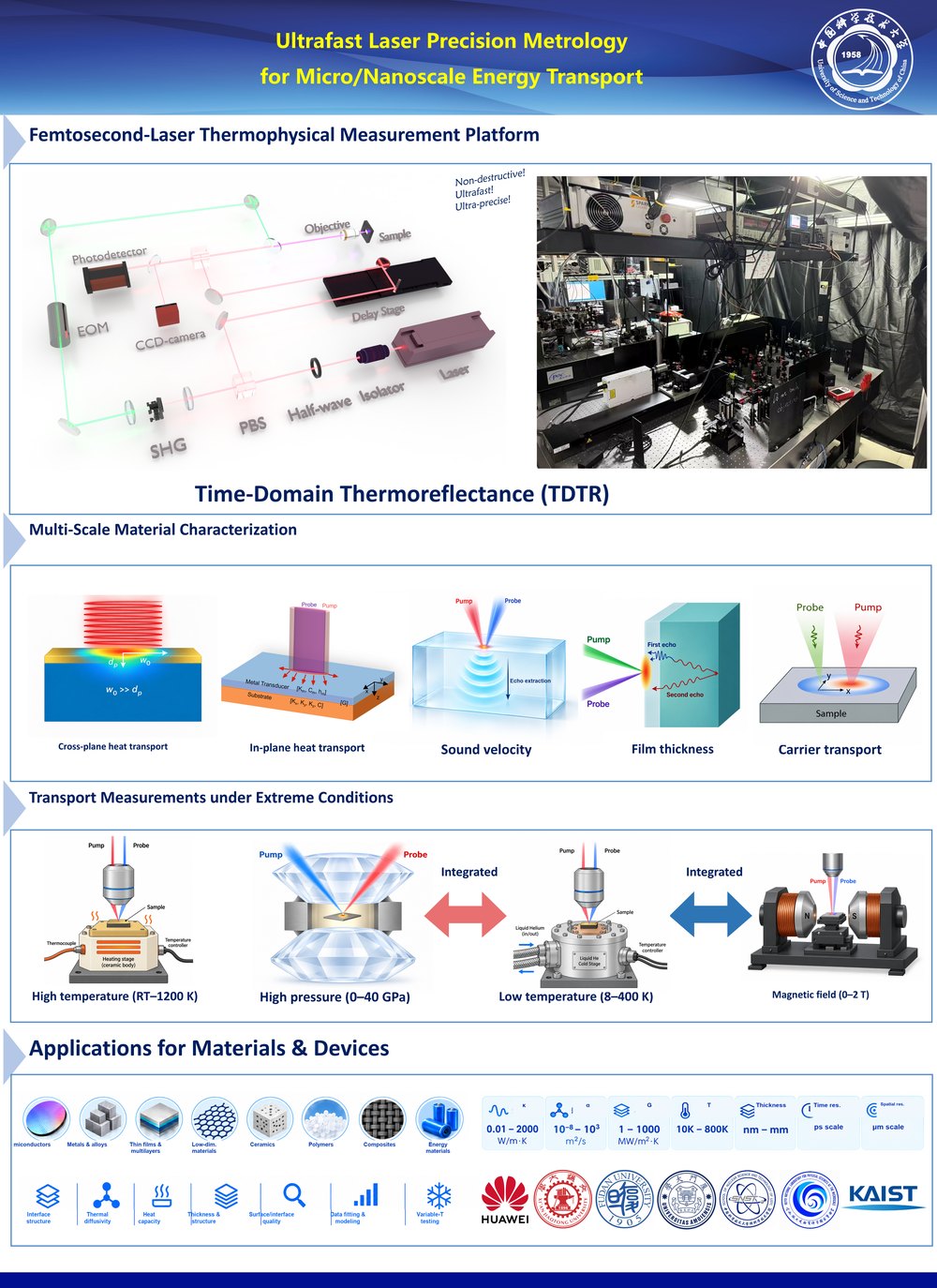
在皮秒-亚微米尺度与高压、高温等极端环境下,原位测量热如何输运。

In-situ measurement of heat transport at picosecond and sub-micron scales, under high pressure, high temperature, and other extreme environments.

自主搭建多平台极端条件热测量能力:(1)超快激光时域热反射(TDTR),皮秒时间分辨、亚微米空间分辨,测量微纳米结构热导率与界面热导;(2)金刚石顶砧(DAC)高压-变温联用平台,实现约 40 GPa 极端压力下热物性原位表征,发现砷化硼高压反常导热(Nature 2022);(3)原位动态热测量,覆盖 DC 至 1 MHz 频率窗口与电场原位调控,追踪器件工作态热输运。测量范围:温度 4–1200 K、热导率 0.1–3000 W/m·K。

We have built multiple platforms for thermal metrology under extreme conditions: (1) Ultrafast time-domain thermoreflectance (TDTR) with picosecond temporal and sub-micron spatial resolution, measuring thermal conductivity and interfacial conductance of micro/nanostructures; (2) a diamond anvil cell (DAC) high-pressure & variable-temperature platform enabling in-situ characterization at ~40 GPa, which uncovered the anomalous high-pressure conduction of BAs (Nature 2022); (3) in-situ dynamic thermal measurement covering DC to 1 MHz with electric-field control, tracking heat transport in operating devices. Accessible ranges: 4–1200 K and 0.1–3000 W/m·K.

Thermal Management: Devices to Systems
04

热管理器件与系统应用

Thermal Management: Devices to Systems

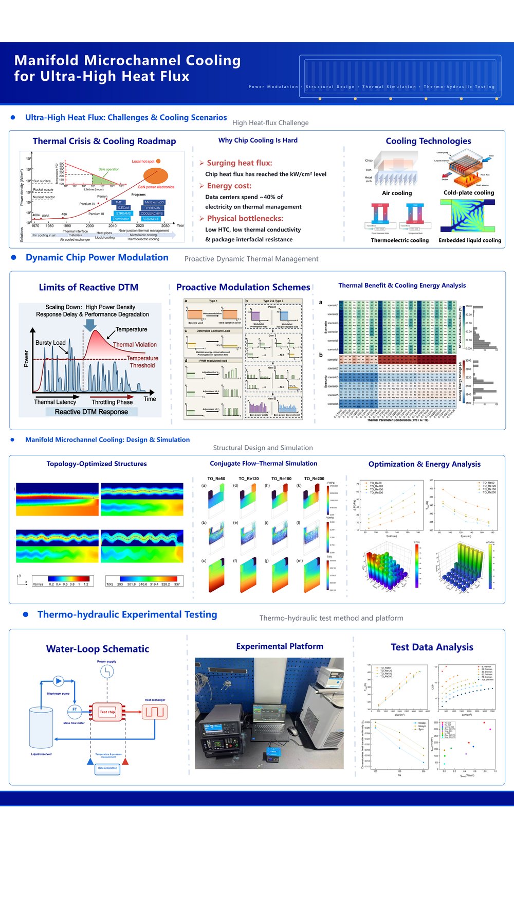
从热开关到芯片冷板,把基础热科学转化为器件与系统的热管理能力。

From thermal switches to chip cold plates, we translate fundamental thermal science into device- and system-level thermal management.

沿“器件→芯片→系统”三个层次发展热管理技术:(1)主动热控器件——国际首创分子热开关,利用电场调控分子化学键实现热流开关比大于 10、响应频率达 1 MHz(Science 2023);(2)芯片级散热——砷化硼衬底使氮化镓功率芯片温升降至 60 K(金刚石 120 K、碳化硅 150 K,Nat. Electron. 2021),砷化硼热界面材料兼具高导热与低模量;(3)系统级热管理——面向数据中心、电动汽车与航天器的多任务动态热管理,结合 PSO/GA/BO 优化与 PWM 智能调控,温度峰值降低约 90%。

We develop thermal management technologies across three levels — devices, chips, and systems: (1) Active thermal control devices — the first molecular thermal switch, using electric fields to tune molecular bonds with an on/off ratio above 10 and response up to 1 MHz (Science 2023); (2) Chip-level cooling — BAs substrates reduce the temperature rise of GaN power chips to 60 K (vs. 120 K for diamond and 150 K for SiC, Nat. Electron. 2021), and BAs thermal interface materials combine high conductivity with low modulus; (3) System-level management — multi-task dynamic thermal management for data centers, electric vehicles, and spacecraft, combining PSO/GA/BO optimization with PWM smart control to cut temperature peaks by ~90%.